

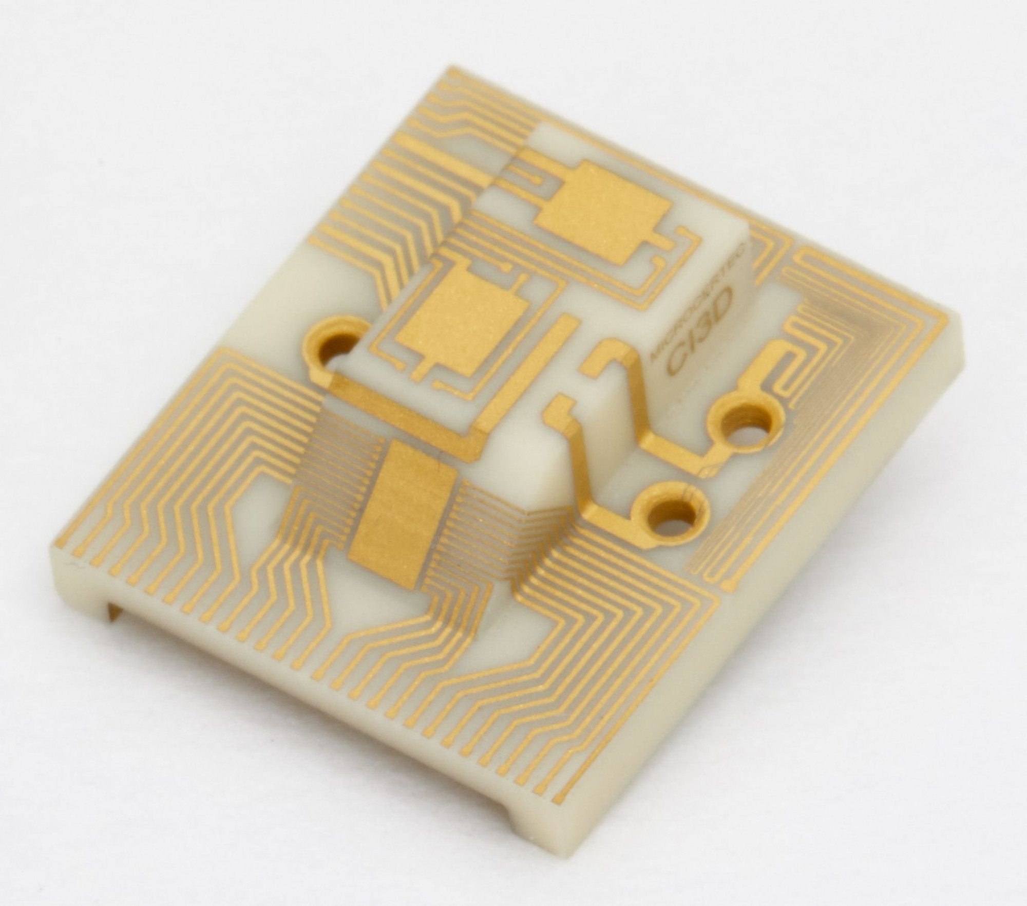
10 years later and a few tens of thousands of 3D-ceramic interconnect devices...
Microcertec, a pioneer in producing this kind of parts
Since the very beginning, Microcertec’s core business in precision machining of technical ceramics has been valued with thin film metallization, the latter being subsequently laser etched to get a 3D-interconnexion circuit. On this 3D-Ceramic Interconnect Device (3D-CID), as in hybrid microelectronics, the customers achieve innovative packaging of components such as MEMS, PIC, CCD,LASER, LED…. for applications requiring functional performances in severe conditions like in airborne systems (inertial navigation system, LIDAR, cooled IR camera…) or in high technology instrumentation (Raman – X rays spectrometry, atomic clock, passive optical network…).
3D-CID has inherited robustness and reliability from hybrid microelectronics and its monolithic design offers freedom in space for component positioning and also mechanical functions to simplify assembly and integration. The concept dates back from the early 90’s when printed circuits on molded plastic benefited from technological improvements. Nowadays, as part of the more recent mechatronic concept, and advances in printed electronics with additive manufacturing technology, it has become popular under the acronym of 3D-MID which stands for 3D-Molded Interconnection Device. Applications include high volume production, mainly in mobile phone (GSM antenna) and automobile (sensors).
From a process standpoint, technical merits of Microcertec lie in the addition of expertise in precision machining of technical ceramics, microelectronics grade thin film metallization and dry laser etching of metallized 3D parts. The result is a flexible technology that fits both rapid prototyping and high quantity production (a few thousands / tens of thousands parts per year). Due to its specificity, the laser process was implemented with in-house expertise and a technical partnership was developed for the metallization. The activity started with a very few customers and turnover but reaches now 10 to 15 % of the company sales. These are nearly exclusively made abroad in niche markets in the field of space, military and civilian aircraft industry, telecommunications, scientific and medical instrumentation.
3D-CID : what benefits ?
As previously mentioned, the main features of 3D-CID’s concept are freedom in component positioning in space and implementation of mechanical functions in order to simplify device assembly and integration relative to shape constraint. The possibility to test the assembly is another benefit. Compared to plastics, technical ceramics along with precision machining are the choice when it comes to require higher mechanical precision and position of components, dimensional stability at high temperature, good electrical insulation and dielectric properties for microwave applications, thermal dissipation (AlN), good surface roughness and metallization quality to achieve reliable chip packaging processes, hermetic feedthroughs or hermetically sealed packaging. The cumulated benefits result in performance gains - improved functionality and reliability, compactness, weight and cost reduction. So, it is not surprising that such a 3D-CID concept is currently used in the seismometer currently in operations on Mars ! (https://www.microcertec.com/microcertec-en-route-for-mars).
3D-CID of the future is emerging
Technical advances involve several processes and technologies. Ultrafast lasers are already available for production and allow high selectivity in removing thin film metallization and also structuring ceramics. This gives access to higher circuit density with line width less than 50µm and pitch smaller than 100µm. Higher resolution of thin traces is also requested for microwave circuits performances where dies are also placed in cavities that are only machinable by such a type of laser. The scope of applications of 3D-CID’s shall also benefit from the advent of the currently emerging additive processes. That concerns both the ceramic body and the interconnection circuit, opening the way to internal structure for ceramics, multilayer design for the circuit with integrated passive components, sensors, via holes, and even printed ribbon wires…. Microcertec is getting prepared to be a technological partner for customers looking for the next generation of 3D-CID.